


Ქმედი ქაღალდის სტანდარტების განსაზღვრა 반도체 გამოყენებისთვის
Ნახევარგამტარების წარმოებაში სუფთა ქაღალდის სტანდარტების სრული გაცნობიერება ძალიან მნიშვნელოვანია, რადგან დაბინძურების დონის დაბალ მაჩვენებელზე შენარჩუნება პრაქტიკულად არის აუცილებელი. ISO კლასების მსგავსმა სტანდარტებმა დააწესეს ლიმიტები იმ მასალების სისუფთავეზე, რომლებიც გამოიყენება სუპერ მგრძნობიარე გარემოში. მაგალითად, ზოგიერთი მწარმოებელი არ განიხილავს ქაღალდს, რომელიც არ აკმაყოფილებს გარკვეულ პარტიკულურ ზღვარს ტესტირების შემდეგ. ეს მიდგმები ნამდვილად განსაზღვრავს სუფთა ქაღალდის არჩევანს სხვადასხვა ამოცანებისთვის მრეწველობის მასშტაბში. კომპანიები მკაცრად ასრულებენ მათ როგორც ხარჯების დეფექტების ასარიდებლად, ასევე იმის უზრუნველსაყოფად, რომ წარმოების ხაზები გაწყვეტილების გარეშე იმუშაოს ყოველდღიურად.
Ნამდვილად სასარგებლოა წმინდა ქაღალდის სტანდარტების დაცვა ნახევარგამტარების წარმოებისას, რადგან ამას დიდი ხელი შეუწყობს პროდუქციის გამომავალში. მრეწველობის ძველ ჩამოყალიბებულ პროფესიონალებს ხშირად აღნიშნავენ, რომ ზუსტად ამ წესების დაცვა ხელს უწყობს პროცესების ეფექტუანობის გაზრდას. თუ დაბინძურების პრობლემები შემცირდება, მაშინ საერთო რენდი უფრო მაღალია, რაც ნიშნავს ნაკლებ დეფექტურ ჩიპებს წარმოების მსვლელობისას. წმინდა ქაღალდის მასალები, რომლებიც გადაკვეთს ხარისხის მკაცრ ტესტებს, არ არის მხოლოდ სასურველი, არამედ აუცილებელია იმ მგრძნობიარე წარმოების გარემოს დასაცავად ისეთი ნამტვრისგან, რომლებიც შესაძლოა მთელი პარტიების დაზიანებას გამოიწვიოს. ნახევარგამტარების წარმომადგენლები კარგად განათლებულნი არიან ამ საკითხში ხარჯების კონტროლის პრობლემების წყალობით, რომლებიც გამოწვეული იქნა ხარისხის დაბალ მაჩვენებლებით.
Კრიტიკული თვისებები: ლინტ-ფรი და დაბალი ნაწილაკების გენერირება
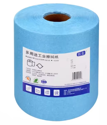
Ნახევარგამტარების წარმოებისას, დასაშვებელია ნამდვილად უხვიანი ქაღალდის გამოყენება, რათა შეინარჩუნოთ პროდუქტის მთლიანობა მთელი პროცესის განმავლობაში. ჩვეულებრივი ქაღალდი ხვდება ბოჭკებს, რომლებიც გავრცელდებიან წარმოების ადგილებში. ეს მცირე ბოჭკები არიან ნამდვილი პრობლემების წყარო პროდუქტის სანდოობის თვალსაზრისით. როდესაც წარმოების დროს ქაღალდიდან გამოყოფილი ბოჭკების რაოდენობა მცირდება, შესაბამისად მცირდება დაბინძურების წყაროები წმინდა ოთახებში. ეს ძალიან მნიშვნელოვანია, რადგან ნახევარგამტარების წარმოება მოითხოვს ულტრაწმინდა პირობებს. უმიკროსკოპიო ნაწილაკებიც კი შეიძლება მთელი ჩიპების სერიის დაზიანებას გამოიწვიოს, ამიტომ წმინდა ოთახების მთლად უხვიანი მდგომარეობის შენარჩუნება აბსოლუტურად აუცილებელია ხარისხის კონტროლისთვის ამ ზუსტი ინდუსტრიის პირობებში.
Ნაწილაკების მცირე გენერირება მნიშვნელოვან როლს ასრულებს ნახევარგამტარების წარმოებისას დეფექტების დასაქვეითებლად. სხვადასხვა ლაბორატორიიდან მოვიდებული კვლევები აჩვენებს, რომ მწარმოებლების გადასვლის შემთხვევაში წმინდა ქაღალდის პროდუქტებზე, ისინი აღიარებენ ჰაერში არსებული ნაწილაკების ნამდვილ შემცირებას. ეს ნიშნავს საერთო დეფექტების შემცირებას. მონაცემები ასევე საკმარისად ნათლად ადასტურებს ამას - ბევრი საწარმო აღნიშნავს გარემოს გაწმენდას გადასვლის შემდეგ. დაბინძურების დონე მკვეთრად იკლებს, რაც ეხმარება მგრძნობიარე წარმოების მოწყობილობების დაცვაში. წმინდა ქაღალდის გამოყენება უფრო კარგად უზრუნველყოფს საწარმო სივრცეში გლუვ პროცესებს. ნახევარგამტარების საწარმოები, რომლებმაც კი მიიღეს ასეთი პრაქტიკები, ხშირად ახსენებენ გამოშვების მოცულობის გაუმჯობესებას და შეჩერების დროის შემცირებას ნაწილაკებთან დაკავშირებული პრობლემების გამო.
Წინადადების მონაცემები: ლოგირება და მონიტორინგი
Class 100 Cleanrooms: მონაცემთა ლოგირება Lint-Free Paper-ზე
Დაბინძურების კლასი 100-ის შესაბამისად დამზადებული წმენდა ოთახებისთვის აღჭურვილობის მონაცემების ჩაწერისას მკაცრი წესების დაცვა აუცილებელია, რაც ხშირად ნიშნავს განსაკუთრებით წმენდა ქაღალდის გამოყენებას ზუსტი და კომპლიანტური მუშაობის უზრუნველსაყოფად. ასეთი სუპერწმინდა სივრცეები, განსაკუთრებით ნახშირბადის გამომცემი ქარხნების შემთხვევაში, საჭიროებს განსაკუთრებით წმენდა ქაღალდის გამოყენებას, რადგან ჩვეულებრივი ქაღალდი ანტაღობს დაბინძურებას, რაც არღვევს მგრძნობიარე გაზომვებს. სამყაროში გამოყენების გამოცდილება აჩვენებს, რომ წმენდა ქაღალდზე გადასვლა მნიშვნულად აუმჯობესებს ჩვენი მონიტორინგის სიზუსტეს და უზრუნველყოფს უკეთეს კონტროლს ასეთ მნიშვნულ გარემოში. ყველაზე გამოცდილი ტექნიკოსები გვეუბნებიან, რომ ყველა რეგისტრაციის დროს გამოვიყენოთ განსაკუთრებით წმენდა ქაღალდი. ეს მარტივი ნაბიჯი ამცირებს სისტემაში არასასურველი ნაწილაკების შეღწევას და ეხმარება კლასი 100-ის მკაცრ მოთხოვნების შესრულებაში დამატებითი შრომატევადობის გარეშე.
Ჰაერის ხარისხის მონიტორინგი მწვერვალი ქაღალდით ნაწილაკების შერჩევით
Ნახშიროვანი მასალების და ნახშირბადის ნანომასალების მწარმოებელი სამეცნიერო-ტექნიკური კონფერენცია და გამოფენა გაიმართება 2024 წლის 11-13 ივნისს ჩინეთის მეცნიერებათა აკადემიის ინსტიტუტის სინყუნის სამეცნიერო პარკში, სინყუნი, ლიაონინგი, ჩინეთი. კონფერენციას მასალების მეცნიერებაში სამეცნიერო კვლევების საერთაშორისო ჟურნალის რედაქცია უმასპინძლებს. ღონისძიება მიზნად ისახავს მკვლევართა და ინჟინრების შეკრებას ნახშიროვანი მასალების და ნანომასალების სფეროში საერთაშორისო ახალი კვლევებისა და ტექნოლოგიების გასაზიარებლად.
Wafer Processing Stages: Precision Protection
Die-Attach Lines: Clean Paper Separation of Diced Wafers
Დიე ატაჩის ოპერაციებში წმინდა ქაღალდე არის მნიშვნელოვანი კომპონენტი დაჭრილი ვეფრების გასაყოფად, რაც აჩერებს მათ დაზიანებას ან დაბინძურებას მუშაობის დროს. გასაყოფი არ იქნება საჭირო, ვეფრები შეიძლება შეხებისას დაიხატონ ან მიიღონ ნაწილაკები, რაც აარიდებს მათ ხარისხს. როდესაც მწარმოებლები წმინდა ქაღალდეს ამატებენ ვეფრებთან მუშაობის პროცედურებში, ისინი მნიშვნელოვნად ამცირებენ ვეფრებს შორის ფიზიკურ კონტაქტს და დამაგრებული მტვრის დაგროვებას მთელი წარმოების ხაზზე. ნახევარგამტარი ფაბრიკების მიერ ამ პრაქტიკის მიღების შედეგად მუდმივად უკეთ მოსავალს აღწერენ, ვინაიდან ნაკლები ვეფრი იბრუხება ან იბინძურდება დამუშავების დროს. წმინდა ქაღალდე უზრუნველყოფს ვეფრების სიწმინდეს მთელი წარმოების მსვლელობისას, რათა უმცირესი კომპონენტები დაემთხვეს თანამედროვე ელექტრონიკისთვის საჭირო მკაცრ სტანდარტებს. ნახევარგამტარი პროდუქციის მწარმოებლებისთვის, რომლებიც უმაღლესი ხარისხის პროდუქტების მიწოდებას უმიზნებენ ნაკლები დეფექტით, ხარისხიანი წმინდა ქაღალდის შეძენა ტექნიკურად და ეკონომიკურად გამართლებულია.
CMP ლაბორატორია: სლარის ნაშრენის შემოწმება გარემოდადების გარეშე
Სუფთა ქ 종ა მნიშვნელოვან როლს ასრულებს ქიმიურ-მექანიკური გასწორების (CMP) ლაბორატორიებში, სითხის ნაშთების შემოწმებისას. მისი გარეშე ყოველთვის არსებობს გამოცდების დროს გადატარების რისკი. ლაბორატორიებმა სუფთა ქაღალდის გამოყენების სტანდარტული პროცედურები შეიმუშავეს, რადგან ის უზრუნველყოფს ზუსტი შედეგების მიღებას და დანარჩენის დაცილებას დამაბინძურებლებისგან. ბევრი დაწესებულება აცხადებს, რომ ნაკლები პრობლემა აქვს დაბინძურებასთან დაკავშირებით, იმის შემდეგ, რაც სისტემატიურად იწყებს ამ მეთოდის გამოყენებას. ნახევარგამტარებთან მუშაობისას, სადაც ხარისხი ძალიან მნიშვნელოვანია, სწორი ქაღალდის გამოყენებით ნაშთის დონეების დაკვირვება და მართვა ყველაფერს განსხვავებულად აქცევს. ამიტომ უმეტესობა გამოცდილი ტექნიკოსების დარწმუნებულნი არიან, რომ სუფთა ქაღალდის მაღალი ხარისხი საჭიროა ყოველდღიური მუშაობისას CMP პროცესებში.
Ფოტოლითოგრაფია და რეტიკლის მართვა
Ჰაზის პრევენციისთვის აკიდის გარეშე თხელი ქაღალდის გამოყენება
Რეტიკელების შესაფუთად მჟავას არ მომცემ და სუფთა ქაღალდის გამოყენება ხელს უშლის ქვეშქარის წარმოქმნას, რაც უზრუნველყოფს მაღალ ექსპოზიციის ხარისხს ფოტოლიტოგრაფიის დროს. ეს რეტიკელები საკმარისად მგრძნობიარე კომპონენტებია და უმცირესი რაოდენობის ქვეშქარიც კი შეიძლება მათ მუშაობას დაარღვიოს, რაც შაბლონების წარმოქმნის პროცესში პრობლემებს იწვევს. სუფთა ქაღალდი იმ მჟავების წინააღმდეგ იცავს რომლებიც ქვეშქარის წარმოქმნას იწვევენ. სპეციფიკაციების განხილვისას, ამ კონკრეტული ტიპის ქაღალდი მნიშვნელოვან ფოტოლიტოგრაფიულ პროცესებში კარგად მუშაობს, რადგან ის არ არის აქტიური სამუშაო პროცესში გამოყენებული საერთო ქიმიკატებთან და აკავებს დამაბინძურებლებს რეტიკელების მიუწვდომლობას. სტუდიებმა სამართლიანად აჩვენა, რომ სუფთა ქაღალდის გამოყენების შემთხვევაში კომპანიები ქვეშქარის დაგროვების პრობლემას თავიდან ასავლენ. ნახევარგამტარების სფეროში მუშაობისას ნათელი ოპტიკისა და ზუსტი შაბლონების შენარჩუნება მხოლოდ სასურველი არ არის, არამედ საჭიროა კარგი წარმოების შედეგებისთვის.
Ტენის კონტროლი რეტიკლების შენახვაში
Რეტიკელების შენახვისას სიტვის კონტროლის შესახებ პრობლემა მნიშვნელოვან როლს თამაშობს, ხოლო წმინდა ქაღალდი მათი დაზიანებისაგან დაცვაში მნიშვნელოვან როლს თამაშობს. ქაღალდი შთანთქავს ზედმეტ ტევს, რაც ხელს უშლის ოქსიდაციასა და კოროზიას, რომელიც შეიძლება ნელ-ნელა დააზიანოს რეტიკელები, თუ უყურადღებოდ დატოვებული იქნება. კვლევები ამას საკმარისად უზრუნველყოფს, რადგან სწორი ქაღალდის მართვა არიდებს ტენიანობას და გაახანგრძლივებს ამ არსებითი კომპონენტების სიცოცხლის ხანგრძლივობას. უმეტესობა იმ ადამიანებისა, ვინც აკადემიურად გაერკვევა ამ საქმეში, სუფთა ქაღალდის გამოყენების რამდენიმე კარგ პრაქტიკას გვთავაზობს ტენიანობის კონტროლის საშუალებით. ისინი საუბრობენ მის სტრატეგიულად მოწყობაზე შენახვის ყუთებში და ხშირად ისინი ამას დამატებით ასუფთავებენ დესიკანტებთან ერთად. როდესაც ყველაფერი სწორად ხდება, ამ ნაბიჯების შედეგად რეტიკელები მუშაობს ზუსტი ფოტოლიტოგრაფიის სამუშაოებისთვის, რაც მნიშვნელოვან განსხვავებას ქმნის ნახევარგამტარი წარმოების სერიებში, სადაც ერთგვაროვნება ყველაზე მნიშვნელოვან პირობას წარმოადგენს.
Ინტერლეივინგის საუკეთეო საფრთხეები იონური მონაკვეთებით
Იმის უზრუნველყოფა, რომ ნივთები მთლად გაწმინდდეს, ძალიან მნიშვნელოვანია ინტეგრირებული სქემების დასაფასობაში, თუ გვინდა დავამარცხოთ ყველა ამ არასასურველი დამაბინძურებელი. გასაგებია, რომ ამ მიდგომის მიღების შემდეგ კომპანიები ხდებიან ლიდერები თავის სფეროში. ამის საშუალებას იძლევა სპეციალური იონური მტვრის ბლოკირების ფენების გამოყენება შუაში ჩადებული გამწმენდი ქაღალდით ერთად. როდესაც მწარმოებლები ამ დაცვის მეთოდებს ერთად იყენებენ, უფრო მაღალი ეფექტურობით ხელი შეუშლიან მტვრის ხელიდან ნაზი ნაწილების დაცვას დასაფასობის პროცესში. არსებობს ამის დამაგრებული მაგალითებიც. ზოგიერთმა ქარხანამ შეატყობინა მნიშვნელოვნად ნაკლები პრობლემის არსებობა დაბინძურების საკითხზე ამ ტიპის ყუთებზე გადასვლის შემდეგ. კერძოდ, ერთ-ერთმა საწარმომ დაფიქსირდა დაახლოებით 30%-ით ნაკლები დეფექტი, რომელიც გამოწვეული იყო მტვრით და ბინძურებით, როდესაც დაიწყო ამ კომბინირებული მიდგომის გამოყენება. ეს სამყაროში ასევე გასაგებია, ვინაიდან უმეტესი ხარისხის კონტროლის მითითებები მოითხოვს საკმარისად მკაცრ სუფთისყოფის სტანდარტებს როგორც დასაფასობის, ასევე ასამბლის ოპერაციების მიმართულებით.
Თანამედროვე ქაღალდე ESD-სენსიტიური კომპონენტების დაცვისათვის
Როდესაც ელექტროსტატიკური განმუხტვის მგრძნობიარე კომპონენტებთან მუშაობთ ტრანსპორტირებისა და მართვის დროს, წინასწრებით დამზადებული ქაღალდი ნამდვილად სასიცოცხლოდ აღმოჩნდება. მასალა აჩერებს ამ არასასურველ ESD მოვლენებს, სანამ ისინი მოახდენენ ზიანს ნაზავზე და მათ შესრულებაზე. უმეტესი მწარმოებლების მიერ წინასწრებით დამზადებული ქაღალდის შეტანა სტანდარტულ ოპერაციულ პროცედურებში კარგი მიზეზით მოხდა. არ არის მხოლოდ დამცავი ფენა კომპონენტებს შორის, ის ნამდვილად ამცირებს სტატიკური დამუხტვის დაგროვებას მოძრაობის დროს ხახუნის გამო. ასევე საკმარისად ნათლად ასახავს საველე შედეგებს, რამდენიმე საწარმომ შემთხვევაში შეატყობინა დაახლოებით 40%-ით ნაკლები პრობლემა ელექტროსტატიკური ზიანის საკითხში წინასწრებით დამზადებული ქაღალდის მეთოდებზე გადასვლის შემდეგ. ამას გასაგები ხდის იმ ტექნოლოგიური კომპანიების დიდ რაოდენობას, რომლებიც ამ მარტივ ამონახსნს უკვე ამ ხარჯიანი მოწყობილობების დასაცავად მიუწვდომელად მიიჩნევენ ტრანსპორტირებისა და შენახვის დროს.
Ინოვაციები ჩистი ქაღალდის ტექნოლოგიაში
Ნანოთბანის მისამართი ჩистი ქაღალდი გამარტივებული წარმოქმნისთვის
Ნანობჭედის ტექნოლოგიაში ბოლო განვითარება გვაძლევს შესაძლებლობას გავუწმინდოთ ქაღალდის წარმოებაზე ახალი კუთხიდან მოვუხილოთ, რადგან ფილტრაციის შესაძლებლობები სიწმინდის ახალ დონემდე მიგვიყანს. რით არის ეს ტექნოლოგია იმდენად განსაკუთრებული? ის საშუალებას აძლევს მწარმოებლებს წარმოქმნან ქაღალდი, რომელიც შეძლებს იმ მიკროსკოპული ნაწილაკების დაჭერას, რომლებსაც ჩვეულებრივი მასალები სრულიად გამოტოვებენ. წარმოიდგინეთ ისეთი ადგილები, სადაც უმცირესი მინარევიც კი მნიშვნელოვანია – პირველ რიგში ნახშირბადის გამტარი ქარხნები მოდის გონში. კვლევები აჩვენებს, რომ ნანობჭედით დამზადებული ქაღალდი შეიძლება დაახლოებით ყველა ნაწილაკის დაჭერა მოახერხოს, ზოგჯერ მიაღწიოს ამ შესანიშნავ 99.99% მარკას. იმ კომპანიებისთვის, რომლებიც ულტრასუფთა გარემოში მუშაობენ, ასეთი სახის მუშაობა მხოლოდ კარგი არ არის, არამედ აუცილებელია. როგორც სხვადასხვა სექტორები უფრო სუფთა პროცესებს უპირებენ, ნანობჭედის ტექნოლოგია უფრო მნიშვნელოვან როლს თამაშობს მკაცრი სტანდარტების დასაცავად.
Რეციკლირებადი მასალები განახლებული მოთხოვნების მიღწევა
Ნახევარგამტართა სექტორი ზრდადი წნევის ქვეშ იმყოფება გამარტივებული გამოყენებისკენ, ხოლო გამეორებადი სუფთა ქაღალდის მასალები სწორედ ის პასუხია, რომელიც ბევრ კომპანიას სჭირდება. ჩვეულებრივი ქაღალდის პროდუქტებიდან ამ უფრო სუფთა ალტერნატივებზე გადასვლა ნიშნავს, რომ ბიზნესები ფაქტობრივად შეამცირებენ გარემოზე გავლენას. ზოგიერთი კვლევა აჩვენებს, რომ ამ ახალი მასალების გამოყენებისას ნახევარი სამი ნაწილით ნაკლები ნარჩენები და ნახევარი სამი ნაწილით ნაკლები ნარჩენები წარმოიქმნება სტანდარტული ვარიანტებთან შედარებით. მწარმოებლებისთვის, რომლებიც მომდევნო წელზე უყურადღებებენ, ამ ეკო-შემეცნებითი მიდგომების მიღებაში ნამდვილად ღირებულება მარაგდება. ისინი აკმაყოფილებენ ამ აბანოებს მომთაბარე წესებს, ასევე საშუალებას აძლევს კომპანიებს ისაუბრონ იმაზე, რომ ისინი პლანეტისთვის მათი წვლილის შესახებ ფიქრობენ. ამ სახის ქაღალდის ტექნოლოგიებში ინვესტირება მხოლოდ გარემოსთვის კარგი არ არის, არამედ ბიზნესის გამართლებაც კი, განსაკუთრებით კი მაშინ, როდესაც მომხმარებლები უფრო მეტად განხილავენ სადგან მოდის მათი პროდუქტები და რა ზემოქმედება აქვთ.
Ხშირად დასმული კითხვები
Რატომ არის თეხნული ქაღალდი მნიშვნელოვანი სემიკონდუქტორულ წარმოებაში?
Თეხნული ქაღალდი არის საგანმანათლეო სემიკონდუქტორულ წარმოებაში, რადგან მისი როლია დახმარება დახრების მინიმიზაციაში. ის დახმარება პროდუქტის ინტეგრიტეტის მართვაში და გამოსახატებლად წარმოების ეფექტიურობის გამარტივება დახრების პრევენციის გამო.
Რა სტანდარტები განმართლებული ქაღალდის განმართვას განისაზღვრობა სემიკონდუქტორების გამოყენებისას?
Განმართლებული ქაღალდი სემიკონდუქტორების გამოყენებისთვის განისაზღვრება სტანდარტებით, როგორიცაა ISO კლასის სპეციფიკაციები, რომლებიც წყაროებში შეზღუდული გარემოებში დაყოვნებულია შესაძლო დაბინძურების დონე.
Როგორ წვდომა განმართლებულ ქაღალდის გამოყენება ESD-სენსიტიური კომპონენტების დაცულებაში?
Განმართლებული ქაღალდი დაცულებს ელექტროსტატიური დისჩარჯის ღონისძიებებს, ფიზიკური ბარიერის როლად მოქმედობით და შემცირებული სტატიკური დაბინძურების გენერირებით, რათა დაცული იყოს კომპონენტების ინტეგრიტეტი.
Რა ინოვაციებია განმართლებული ქაღალდის ტექნოლოგიაში?
Წმენდის ქაღალდის ტექნოლოგიებში გამოჩნდა ნანოძაფის ბაზაზე დამზადებული ქაღალდე მაღალი სიწმინდისთვის და გამეორებით გამოყენებადი მასალები, რაც აკმაყოფილებს გამძლეობის მოთხოვნებს.
Სარჩევი
- Ქმედი ქაღალდის სტანდარტების განსაზღვრა 반도체 გამოყენებისთვის
- Კრიტიკული თვისებები: ლინტ-ფรი და დაბალი ნაწილაკების გენერირება
- Წინადადების მონაცემები: ლოგირება და მონიტორინგი
- Wafer Processing Stages: Precision Protection
- Ფოტოლითოგრაფია და რეტიკლის მართვა
- Ინტერლეივინგის საუკეთეო საფრთხეები იონური მონაკვეთებით
- Თანამედროვე ქაღალდე ESD-სენსიტიური კომპონენტების დაცვისათვის
- Ინოვაციები ჩистი ქაღალდის ტექნოლოგიაში
-
Ხშირად დასმული კითხვები
- Რატომ არის თეხნული ქაღალდი მნიშვნელოვანი სემიკონდუქტორულ წარმოებაში?
- Რა სტანდარტები განმართლებული ქაღალდის განმართვას განისაზღვრობა სემიკონდუქტორების გამოყენებისას?
- Როგორ წვდომა განმართლებულ ქაღალდის გამოყენება ESD-სენსიტიური კომპონენტების დაცულებაში?
- Რა ინოვაციებია განმართლებული ქაღალდის ტექნოლოგიაში?